As semiconductor device power density rises (SiC, GaN, high-performance CPU/GPU), traditional thermal materials —pure copper (400 W/m路K) and aluminum (200 W/m路K) —can no longer keep up. Diamond-copper composites combine diamond's ultra-high thermal conductivity (1200—200 W/m路K) with copper's processability, achieving 600—50 W/m路K —twice that of pure copper. This makes them ideal for high-power chip heat spreaders and substrates.
⚠️ This article is an educational overview of coarse-grained diamond applications in copper composites for semiconductors. DIAMTECH specializes in PCD-grade ≤20μm diamond micron powder; coarse grades described here are not our standard products.
Why Diamond + Copper
Diamond is the most thermally conductive known material. Its thermal conductivity comes from phonon transport in a nearly perfect covalent lattice. Copper is an excellent conductor (400 W/m路K), machinable and affordable. Their combination yields a material that: (1) conducts heat twice as well as pure copper; (2) has a tunable coefficient of thermal expansion (CTE) matched to semiconductor materials SiC, GaN, GaAs; (3) retains mechanical strength and machinability.
Semiconductor Applications
- Heat spreaders for high-performance CPU/GPU and AI accelerators
- Substrates for microwave integrated circuits (microwave modules, phased array antennas)
- Heat sinks for SiC/GaN power electronics (EVs, charging stations)
- Laser diode and optoelectronic packages
- Thermal interfaces in high-density chip packages (chiplet, 3D packaging)
Fabrication Methods
| Method | Principle | Advantages | Disadvantages |
|---|---|---|---|
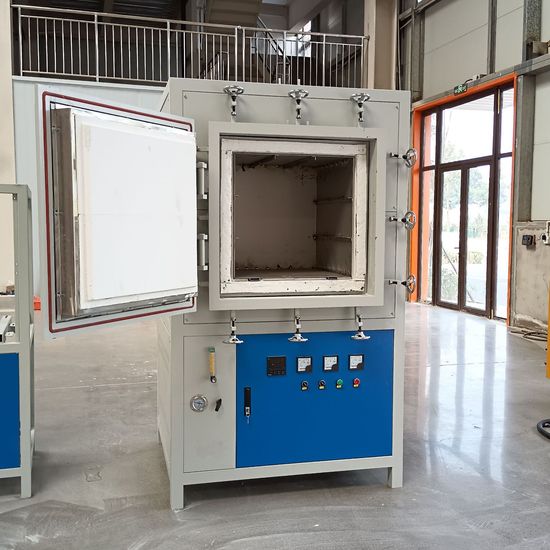
| High pressure (HPHT) | Sintering under 3— GPa, 1000—500°C | High density, diamond skeleton formation | High cost, complex shapes limited |
| Vacuum hot pressing | Hot pressing in vacuum, 800—000°C, 20—0MPa | Good surface quality, controlled density | Limited shapes, long cycle |
| Melt infiltration | Infiltration of porous diamond preform with molten copper under pressure | High thermal conductivity, near-full density | Complex equipment, precise temperature control |
| Spark plasma sintering (SPS) | Pulsed current + pressure, 900°C, 30MPa, 20min | Fast cycle, fine grain, high density | Limited part sizes |
Key Problem: Interfacial Thermal Resistance
The main obstacle to practical diamond-copper composites is poor wettability of diamond by copper. Diamond is chemically inert, copper does not wet its surface, leading to high interfacial thermal resistance. Even at high diamond volume fractions (50—0%), without interface modification the composite thermal conductivity remains low due to broken thermal pathways.
Solution: Diamond Surface Metallization
Carbide-forming metals (Ti, Cr, W, Zr) are coated on the diamond surface, forming a carbide interlayer (TiC, Cr₃C₂ WC, ZrC) upon annealing. This layer chemically bonds to diamond on one side and is well-wetted by copper on the other. Typical coating thickness is 200 nm —1 渭m. Without this modification, achieving thermal conductivity above 400 W/m路K is practically impossible.
Market Outlook
The diamond-copper composite market is growing rapidly, driven by rising semiconductor device power. Industry estimates say demand is driven by power-module, server-optics and high-performance-computing makers across regions. For diamond powder producers, this opens a fast-growing new segment: coarse-grain diamond (50—00 渭m) with surface modification for composites.
Why Matched Thermal Expansion Matters
A heat spreader works in pairs with the semiconductor die, and if the materials' coefficients of thermal expansion do not match, heating and cooling build cyclic stress in the thin solder joint. Over time this causes fatigue, cracks and device failure. Silicon's expansion is about four, silicon carbide about four and a half, while pure copper's is nearly four times higher. That is why pure copper, despite excellent conductivity, is a poor choice for high-power chips. In a diamond-copper composite, diamond fraction acts as a lever: raising it lowers the net expansion and tunes the material to the die without giving up copper's convenience. This is the main reason engineers choose the composite over the pure metal.
Grain Shape and Packing
The practical conductivity depends not only on diamond fraction but on how particles pack. Well-rounded, near-spherical grains pack more densely and allow a high diamond fraction without losing copper flow. Sharp flaky particles, on the contrary, cause interlocking, raise residual porosity and lengthen indirect heat paths. That is why composites call for not just a given size but a narrow particle-size distribution with selected shape. Coarse fractions from fifty to three hundred micrometers are often combined in a bi-modal blend: fines fill gaps between coarse grains, pushing overall diamond share above what one fraction yields. For a powder supplier this means controlling not only the median size but also the upper end of the distribution.
Typical Buyer Questions
How does diamond/copper differ from hexagonal boron nitride?
Hexagonal boron nitride is used as a filler in plastics and ceramics for flexible boards. It conducts heat but far less than diamond, and is usually loaded into a polymer matrix. Diamond-copper is a dense metal for rigid spreaders. The choice is set by required stiffness, operating temperature and budget.
Can I skip modification if I use the highest diamond fraction?
No. As long as copper does not wet the surface, raising diamond fraction only enlarges the area of non-contacting boundaries. Experience shows that without metallization, even at high diamond content, real conductivity stays at pure-copper level or below.
What grain size to choose for a composite?
For metal matrix composites the typical sizes are around fifty to three hundred micrometers with a narrow distribution. The exact size depends on spreader thickness and the chosen sintering route; for bi-modal blends we tune the coarse-to-fine ratio.
How to Choose a Powder Supplier for Composites
Not every diamond powder suits metal matrix composites. What matters here is not purity alone but surface predictability: if carbide layer thickness and composition drift batch to batch, the technologist cannot reproduce conductivity. Before launching series work, ask the supplier for three things: a particle-size certificate with D10, D50 and D90, grain-shape data, and a report on the applied coating. A trial batch from 1 kg remains the first step: on it you check both wettability and how the powder behaves through your sintering cycle. For mass production, lock the recipe and source batch so the fifth shipment repeats the first trial.
Brief Conclusion
Diamond-copper composite fills the niche where pure copper falls short: it needs double conductivity at a CTE matched to SiC and GaN, with acceptable mass. Its practical realization rests not on diamond itself but on the interface: without carbide-forming metallization and bi-modal packing, high figures stay on paper. We supply diamond powder in the 50—00 micrometer range with a controlled surface and back every batch with a report. Start with a trial batch from 1 kg to check wettability and thermal behavior on your own process route.
Need diamond powder for your project?
From 1 kg, standard W5/W10/W20 in stock —48h shipping. Custom fractions 3–7 days. Trial batch — from 1 kg.
Request a trial batch and a quote